Ask A Motion Control Engineer
Complex Motion Challenges Made Simple
Have a tough motion application you’re trying to figure out? Wondering what the best actuator, motor, or motion control solution is for your system? We can help you with:
- Product Demonstrations (live or virtual)
- Sizing and Selection Assistance
- Engineering Consultations
- Proof of Concepts
- Custom Solutions for OEMs
We’ll Help You Ask The Right Questions
To get the most out of your request, our motion engineers will typically ask the LOSTPED questions:
- Load: What are you moving (mass, payload, Center of Gravity)?
- Orientation: Horizontal, vertical, or angled?
- Speed: What are your target speed and accelerations or decelerations?
- Travel: What’s the stroke length or range of motion?
- Precision: What’s the repeatability or accuracy requirement?
- Environment: Temperature, dust, moisture, or cleanroom rated?
- Duty Cycle: Continuous or intermittent? How often is it moving?
Not sure about all of these? No problem — our experts will help you fill in the gaps!
Want to speak with a motion control engineer? Fill out the form below:
What Happens After You Submit?
- Engineer Follow-Up: A Valin engineer will review your information and reach out within a business day.
- Discussion & Refinement: We'll schedule a short meeting (remote or in-person) to clarify your needs.
- Mitigate Risks: We’ll help you figure out how to mitigate risks through demonstrations, proof-of-concepts and experience.
- Documentation & Support: If your project calls for it, you will receive drawings, Bills-of-Materials, videos and support for implementation.
Prefer to Talk Now?
Call us at 800-774-5630 or email CustomerService@valin.com
Q & A
If the proof-of-concept is focused on motion performance, then graphs from the motor’s encoder can be provided. Other tests may include external sensors or video recordings.
Yes! If you have hardware specific to your application, then we can consider using that in our testing.
The most common motion control mistakes we see in machine design are when people:
- Under-size motors and mechanics
- Under-design the machine base so it is flimsy an vibrates to much
- Do not provide enough inputs & outputs
- Do not include the software needed for programming the controls
- Skip good electrical design installation practices such as grounding and shielding
 Macnaught's
 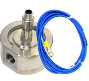 Macnaught's
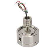
 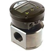 Macnaught's latest hazard offering allows for non-powered hazard meter application. Perfect for remote locations or areas where power is not available. The MX Meter is mated with Macnaught's Simple Apparatus PCB and meets all global intrinsically safe areas.
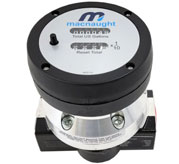 Macnaught's long standing